Electromagnetic (EM) simulation involves using computational models to predict how electric and magnetic fields interact with various materials, components, and structures by solving Maxwell’s equations. Instead of relying on physical prototypes, we can employ these simulations to analyze and visualize how electromagnetic waves propagate and behave in complex environments. This approach streamlines the design and optimization of a wide range of technologies, including antennas, circuits, sensors, optical systems, and common applications such as Wi-Fi networks and MRI scanners.
EM Simulation
The typical EM simulation set up is illustrated in the figure below.
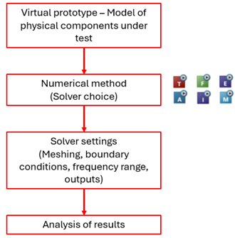
The first step involves creating a virtual model of physical components to be tested. This model should accurately capture the geometry, materials, and relevant features of the device or structure under study. The fidelity of the virtual prototype directly affects the reliability of the simulation results; therefore all critical dimensions, interfaces, and material properties should be carefully defined.
In the second step, an appropriate numerical solver has to be selected to simulate the problem. This choice determines how Maxwell’s equations will be solved for the computational domain and directly impacts simulation accuracy, computational time and memory requirements. The selection depends on factors like geometry complexity, frequency range, material properties, and type of analysis (scattering, radiation or coupling).
In the third step, simulation parameters like global and local mesh properties, boundary conditions, frequency range of the computation and required output parameters are defined. In the final step, post processing is performed for the results to examine the behavior of the computational domain.
Types Of Outputs From EM Simulations
From the EM simulations, we can generate a variety of outputs which reveal the physical behavior, performance and limitation of the physical system under consideration. The following section outlines the key types of outputs commonly obtained from EM simulations and their significance in design and analysis.
Electric And Magnetic Field
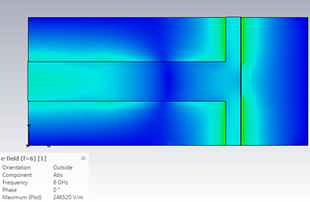
This shows the electric (E) and magnetic (H) field distributions throughout the computational domain. It helps in visualizing where fields are concentrated or leaking, identify hot spots or nulls, and understand coupling or radiation behavior.
S-Parameters (Scattering Parameters)
This is a matrix that shows how an input signal is reflected or transmitted between different ports of a device. If x1 and x2 are the input signals and y1 and y2 are the output signals in a two- port network, the general S parameters are represented by the equation below.

Here, S11 and S22 are the reflection coefficients at ports 1 and 2 respectively. S12 and S21 are the transmission coefficients. Calculating these S parameters is critical for matching circuits and ensuring maximum power transfer with minimal reflection.

Nearfield And Farfield Radiation Patterns
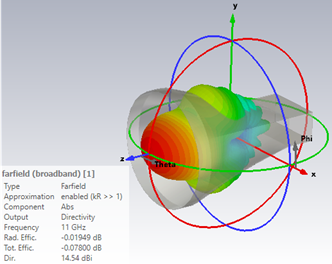
The nearfield region exists close to the source typically within a few wavelengths. It is characterized by strong, reactive electric and magnetic fields that do not radiate energy efficiently but instead store and exchange it between components. Analyzing near-field distributions helps in understanding coupling effects, field confinement, and potential interference with nearby structures or circuits.
The far-field region represents the area sufficiently distant from the source, usually several wavelengths away where the fields transition into radiating waves that carry energy outward. Here, the electric and magnetic fields are perpendicular to each other and to the direction of propagation, forming a well-defined radiation pattern. Far-field distributions are used to evaluate key performance metrics such as antenna gain, directivity, beamwidth, and side-lobe levels, indicating how effectively energy is transmitted in specific directions.
Impedance And Admittance Characteristics
Impedance and admittance characteristics describe how an electromagnetic structure responds to applied electrical signals in terms of voltage and current relationships. Impedance (Z) represents the opposition a device presents to the flow of alternating current, while admittance (Y) is its reciprocal, indicating how easily current can flow. In electromagnetic simulations, these parameters are typically evaluated at input and output ports to assess how efficiently energy is transferred between components or radiated into free space.

By examining impedance versus frequency plots, we can identify resonant frequencies, where the reactive components (inductance and capacitance) balance out, and matching conditions, where maximum power transfer occurs with minimal reflection.
Power Loss And Heating
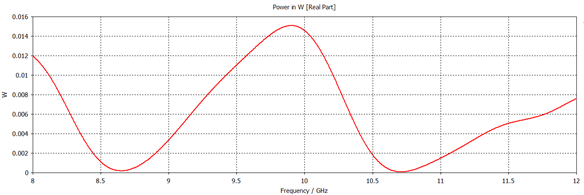
Power loss and heating in electromagnetic simulations refer to the dissipation of electromagnetic energy as heat within materials due to resistance, dielectric, or magnetic losses. When electromagnetic fields interact with conductive or lossydielectric materials, part of the energy is absorbed instead of being transmitted or radiated, leading to ohmic losses (in conductors) and dielectric losses (in insulating materials). This absorbed energy manifests as localized temperature rise which can affect performance, reliability, and safety. EM simulation tools quantify these losses by calculating parameters such as power density, loss tangent, and specific absorption rate (SAR).
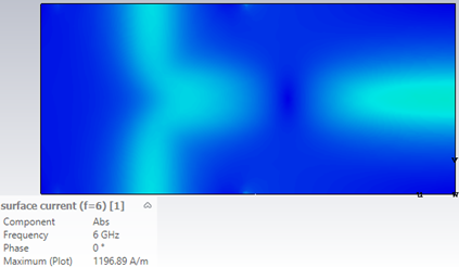
Current And Charge Distributions
Current and charge distributions illustrate how electric current and charge density are spread across the surfaces or volumes of conductive and dielectric materials within an electromagnetic system. These distributions provide deep physical insight into how a device operates, revealing the paths through which energy flows and accumulates.
Resonant Frequencies And Mode Shapes
This describes how and at what frequencies an electromagnetic structure naturally stores and oscillates energy. A resonant frequency occurs when the stored electric and magnetic energies in a system are balanced leading to maximum field amplitude for a given excitation. At these frequencies, the system supports specific field patterns which are known as mode shapes. These mode shapes define how the electric and magnetic fields are spatially distributed within the structure. These modes are determined by the geometry, boundary conditions, and material properties of the components.

Final Thoughts
Electromagnetic simulations provide a powerful tool for analyzing and optimizing the behavior of complex devices without relying on physical prototypes. By accurately modeling geometry, materials, and boundary conditions, and selecting the appropriate numerical solver, we can predict electric and magnetic field distributions, S-parameters, radiation patterns, impedance characteristics, power loss, and resonant behavior. These outputs give deep insight into device performance, highlight potential issues such as hotspots or unwanted coupling, and guide product improvements.
We’re always here to help, so if you have questions about Electromagnetic simulations using CST Studio Suite, or just FEA in general, don’t hesitate to reach out!
